Earlier it was shown how Linux Kernel Development is being overwhelmed by the success of Free Software. This success is mostly due to mass-volume ARM-based products using the Operating System known as "Android", and most devices are either GPL-violating or are effectively Closed Development Projects by virtue of late and fait-accomplit (i.e. legally correct but otherwise pointless) GPL Compliance.
The Software Development Model for ongoing Linux Kernel Development is therefore in danger of being completely overwhelmed, where the extreme number of necessarily-diverse processors and associated platform files is only going to increase. Even the introduction of the new "device tree" system, which places the hardware layout into an external boot-time configuration file, does not help, if the platform's devices being added have to be completely unique on a per-device basis! (Device Tree only helps with code re-use if there are actually any bits of platform hardware which are actually non-unique across multiple devices. sadly this is almost never even realistically practical, in the ARM embedded world).
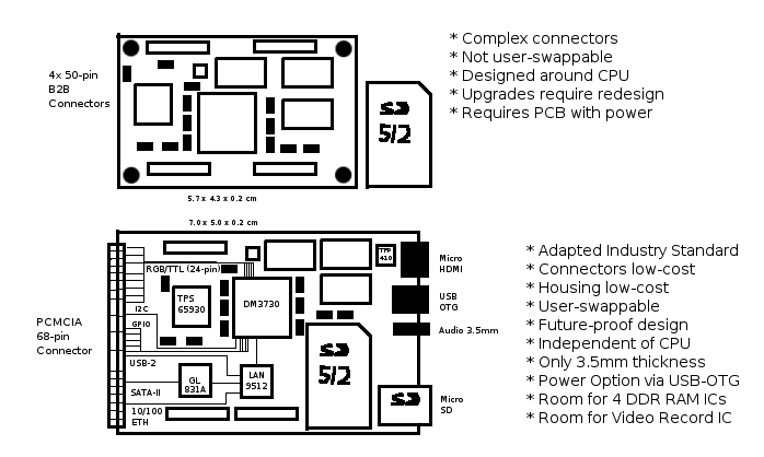
Thus, if the problem is that there is too much diversity, then the solution is clear: reduce the diversity. The best way to do that is to create a de-facto Industry Standard, based around a Star Network (Hub) Standard. On one side of the standard is the CPU, RAM and NAND Flash (along with some complex peripherals that have Micro-connectors associated with them) and on the other side is peripherals, most of which are multi-bus (e.g. USB). The associated Linux Kernel Drivers can therefore be re-used across a wide range of hardware platforms, and, importantly, there is an upgrade path for future processors to be introduced - all with a minimum of fuss.
This article therefore outlines a simple Modular User-upgradeable Architecture, suited to small so-called "embedded" processors, and providing some illustrated examples - Engineering Board, Tablet, Laptop and so on - which demonstrate that the concept is perfectly feasible, at least for mass-market devices (satisfying the high-end "Server" Market at the same time has proven awkward unless the cost of the mass-market devices is also increased. clearly, this is undesirable, so it is best to wait 3 to 5 years before re-evaluating the Modular concept to include MIPI, SATA-III, USB-3, 1000 Ethernet, PCI-e and so on, all of which are ultra-high-speed Buses that are simply not present on the vast majority of today's ARM and MIPS embedded CPUs).
The basic principle is straightforward, and relies critically on the fact that so-called "embedded" processors are small (a large one is 25mm x 25mm), very low power (often well below 1 Watt), and so will easily fit into a small metal shielded box acting as its heat sink, using passive cooling only.
Within this quite straightforward architecture there is a great deal of room for flexibility and future-proofing:
So, despite these interfaces being "Lowest Common Denominator", startlingly it is clearly evident that they're perfectly sufficient for mass-volume purposes, and they've all been around, including SATA, for well over a decade. (SATA however simply was too high-speed for early ARM processors of the time, which were still, a decade ago, running at a whopping 75mhz. To save power, early ARM processors often deployed CF - aka IDE aka PATA - instead, up until even as recently as 2008 with the Samsung Cortex A8 S5PC1xx series, supporting up to UDMA Mode 5 - again, to save power).
Also, from a Software (Device Driver) perspective, sharing of code becomes mandatory. Bear in mind that many manufacturers of ARM-based devices choose an arbitrary CPU, arbitrarily allocate GPIO pins to different purposes and so on, all of which is absolutely essential to be hard-coded into device-specific platform files! and for what - to create yet another identical-looking tablet? With the above approach, it becomes possible to create just the one tablet "chassis", and for users to purchase the PCMCIA CPU card according to their choice and budget. and to remove that CPU card and insert it into an alternate chassis, with the advantage that they carrying their familiar applications and all-important data over to the newer device with no loss of continuity.
Here is a list of possible devices, all of which clearly can be seen to require no more than USB2, SATA-II (if at all), 10/100 Ethernet (if at all) and 24-pin RGB/TTL:
Each of these devices is well worth going over in detail, but each of them is nothing special: for mass-volume purposes they all require nothing more than USB2, SATA, 10/100 Ethernet etc. Bear in mind that the PCMCIA Card itself has additional space for the high-speed connectors such as Micro-HDMI, Micro-USB-OTG, Micro-SD and possibly Video In/Out and possibly Audio In/Out as well. The combination of the Interfaces available to each PCMCIA CPU Card as well as those on the Motherboard therefore brings each combination up to acceptable mass-volume specifications expected for each device.
This example PCMCIA card was designed to demonstrate that Kitarm's DM3730 "module" clearly can be adapted into the PCMCIA form-factor, with ample room to spare. The only disadvantage of this particular design however is that, due to the inclusion of a full-sized SD/MMC Slot (which is technically possible), re-use of existing off-the-shelf and therefore low-cost PCMCIA metal shields would clearly not be possible.
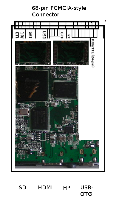
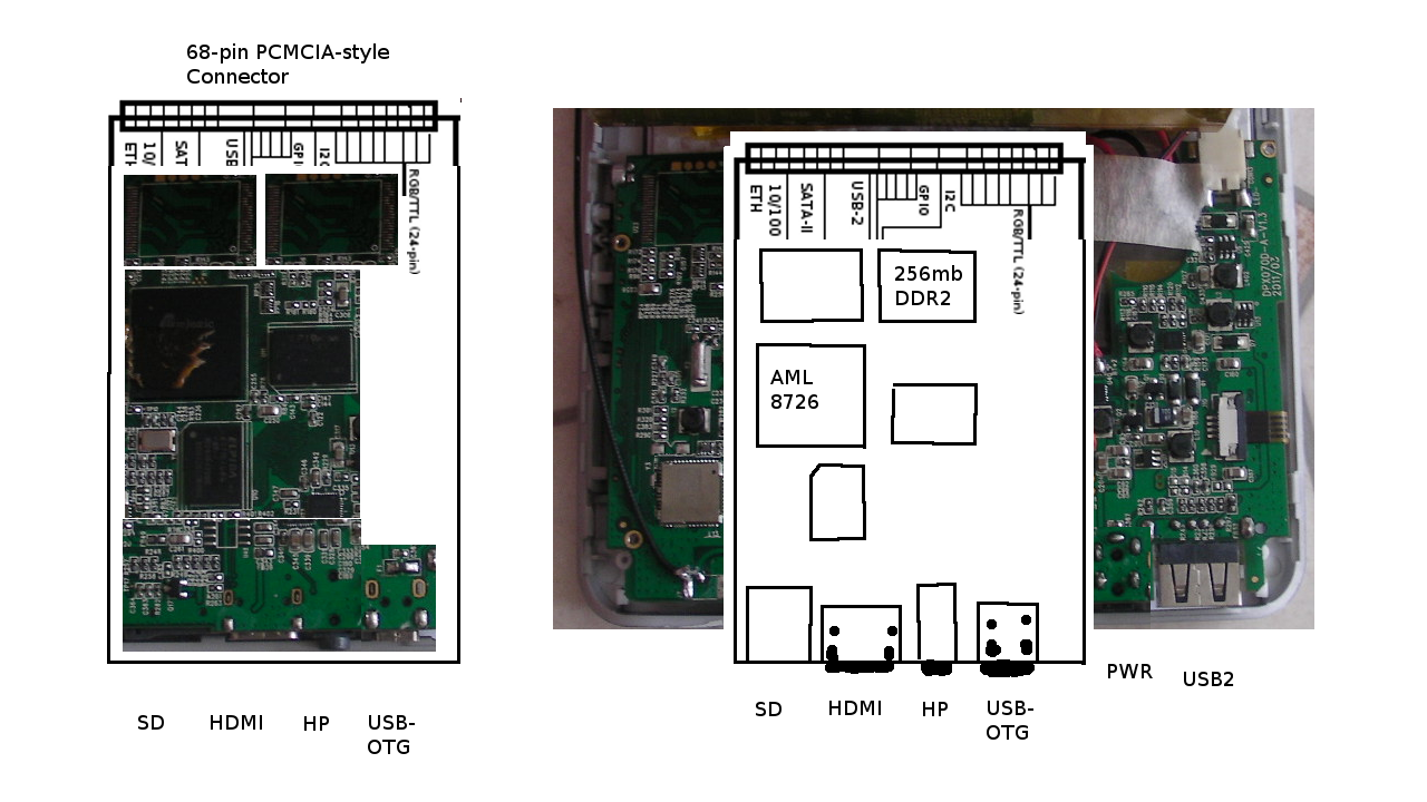
This example PCMCIA CPU card's layout was taken from examining the PCB of a 7in tablet with an AML-8726-M 800mhz Single Cortex A9 CPU. Within the blank space (right centre) is plenty of room for unpopulated Expansion Headers, for "Engineering Purposes". There is also even room for a 2nd Micro-SD slot (again, with the proviso that in mass-volume usage that Micro SD card would obviously be inaccessible, as it would be underneath an off-the-shelf low-cost metal shield).
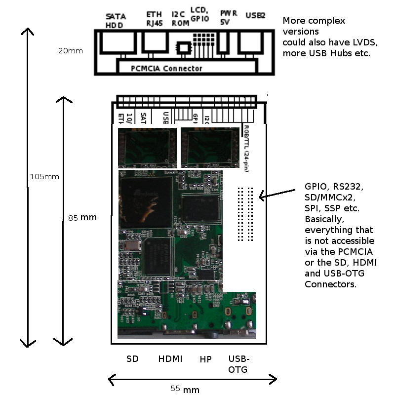
The absolute minimum Engineering Board comprises a PCMCIA CPU card with a tiny 55mm x 20mm PCB that has nothing more than 5V Power and other connectors. Access to the 24-pin RGB/TTL Interface, as well as the 10 GPIO pins, is available via an unpopulated Expansion Header. Bear in mind that this "Micro" Engineering Board, which would cost well under $5 to make and could even be made by an Electronics Enthusiast, can be utilised with any compatible CPU Card.
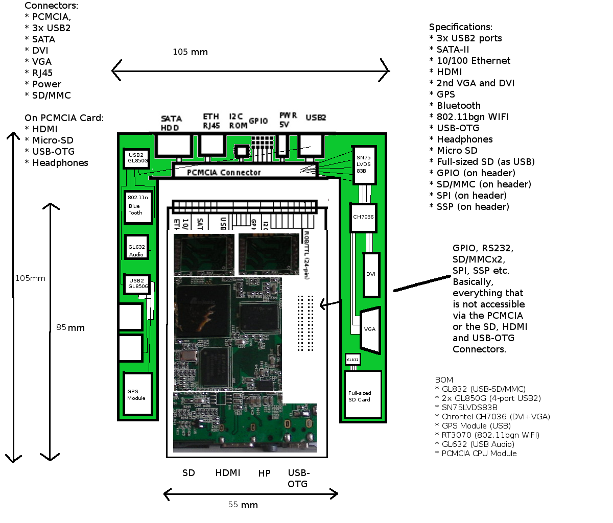
This "Engineering Board" is the usual "Complete Overkill Kitchen Sink" board. Designed to be accompanied with its CAD/CAM Schematics, it's the purrfikt way for the average engineer to perform cut/paste jobs in order to create the customer's desired product.
These are becoming hard to justify but that isn't going to stop Chinese Companies from Having A Go. It's therefore necessary to demonstrate that the PCMCIA CPU Card Concept actually fits inside even the lowest-of-the-low, the 7in tablet, with room to make improvements such as reducing the thickness. Here is the first image, showing a cut-away from a standard 7in Tablet, replacing the space with the exact same CPU but this time on a PCMCIA card:
The next question that came up was that the PCMCIA Socket would be "too thick". So an Assembly was located that proved otherwise: another is here and another set of guide rails also located, which would be a cheaper option but would make user-removable of the PCMCIA CPU card somewhat challenging. Both the Tyco Electronics and FCI assemblies come in versions with a maximum height of 6mm, and the non-eject guide rails from FCI also have a low-clearance part number, 72791-001MLF which will again easily take a 5mm-height PCMCIA Card.
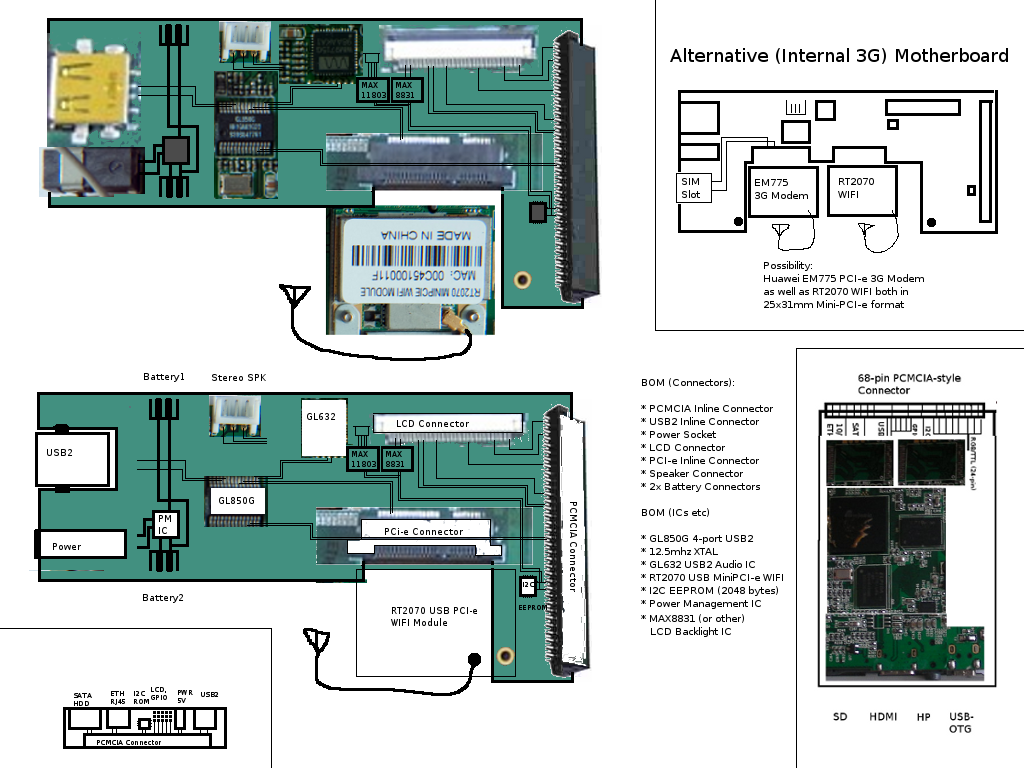
A quick mock-up of a matching motherboard was then created, which shows that there really isn't very much to these PCBs (as anyone who has seen the schematics for the original Hardkernel ODroid can attest. yes, those photos really are it: yes, the majority of the PCB is completely empty). For this 7in Tablet Motherboard, its length is dictated, as with the ODroid, by the size of the device: it must stretch to provide the USB and Power Sockets on the left size. Also, rather than force the PCB Designers to have to get involved with RF, deployment of a Mini PCIe (USB) connector was recommended.
Suitable WIFI parts include the RTL8191SU which is an 802.11abgn 30x26mm USB mini card. Also, an example motherboard (top left) was done which shows how a 2nd Mini PCIe slot can be added which houses a 3G Modem. Kitarm's DM3730 Tablet also follows this principle, showing how use of an inline Mini PCIe connector saves precious height clearance, even when these Mini PCIe 3G and WIFI cards are only 5mm high. (bottom left is the familiar minimalist "Engineering Board").
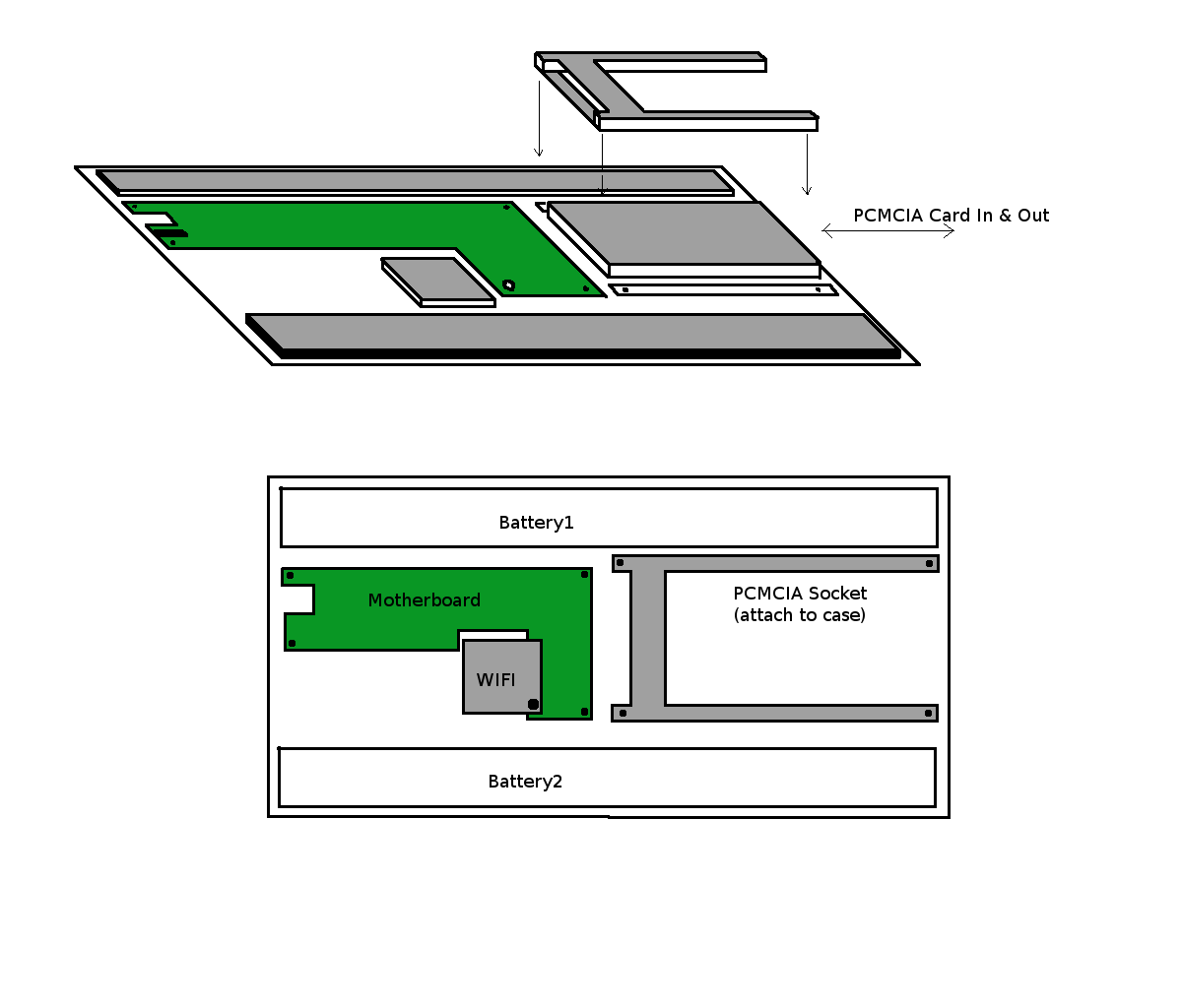
Additionally, concerns were raised about the balance of the device due to battery weight vs PCMCIA CPU card. A design was therefore created which uses two batteries. This resulted in a reduction of the required battery's thickness, from 4mm down to 3mm, whilst also maintaining the same power. A quick isometric drawing was done which shows the principle. Also, it can be seen that the PCMCIA Housing is not attached to a PCB: it's mounted directly onto the tablet's case, saving around 2mm of clearance in the process.
It should, by now, be very clear that if a 7in tablet under 12mm in thickness can be achieved, which has the LCD in the same package as a 5mm PCMCIA CPU Card, a Laptop should be even easier. Such sexy-looking slimline laptops such as the Asus UX Series could easily be reduced in width and weight, even further. Ironically, the risk is that the weight be so reduced, due to the lower power requirements of ARM processors, that the battery becomes so small that there is insufficient weight to keep the device upright!
The only real practical issue is, therefore, to locate a suitable case. Attempting to design a new one, from scratch, is complete insanity unless a budget of $USD 150,000 is available, and a ready-made market guaranteed to purchase 100,000 units. This mistake is why so many early ARM Reference Design Laptops failed: the R & D costs of $250,000 meant that they would only be bought in mass-volume quantities, and even then the prices remained high and uncompetitive against equivalent Intel Atom systems.
So the lesson is clear: re-use an existing case, until such time as mass-volume sales actually come along, in the form of an actual order for 100,000 units. Then it's okay to spend an average of $USD 1 per unit to make a nice pretty case.
More information and details on what is involved, as well as the background, can be found here.
These are merely cut-down versions of the Monster Engineering Board. Possibly the best modular design here is to deploy multiple Mini PCIe USB Slots, internally, as there are even Mini PCIe USB DVB-T cards, available under multiple confusing re-branded names. The Yuan MC770A is especially noteworthy because it's supported under Linux. The LinuxTV page for DVB-T USB Devices even has the MC770A listed as working by default since the 2.6.30 Linux Kernel.
Other peripherals which will work well in this Mini PCIe USB form-factor include, as mentioned in the 7in tablet section above, the 3G Modem as well as the 802.11abgn WIFI Cards. A company called BPlus maintains an excellent Compatibility List with tested devices in an excellent low-cost adaptor called the USBMA. This adaptor also has the schematics needed to show PCB Engineers how to link up the SIM Cards required for 3G HSDPA Modems.
The only risk with these Mini PCIe USB Cards is that many people make the unfortunate mistake of purchasing a PCIe card, and expect it to work. To be frank: given that a screwdriver is required to open up these boxes, that's an acceptable risk.
The PCMCIA form-factor is small enough, and USB and 10/100 Ethernet sufficiently ubiquitous, so that pretty much any mass-volume device can be converted. This includes:
It can be seen, therefore, that there really isn't much in the way of mass-volume computing appliances that can't be adapted to this modular architecture. To fit into that small list, it's necessary to require multiple fast SATA drives (i.e. where USB-to-SATA adaptors will not do), or to have multiple 10/100 Ethernet Ports (where an on-board Hub or multiple USB-to-Ethernet adaptors will not do), or to have Gigabit Ethernet, or to have an Intel or an AMD Processor, or to have monster 3D Graphics (consuming 6 to 150 watts), or to have a full PCI express interface.
Whilst this is quite a long list, it leaves a great deal of computing technology which is still perfectly adequate - and desirable.
Virtually all modern computing appliances can be adapted to a Modular Computing Architecture form-factor, re-using existing assemblies, housings and case-work that is mass-produced, in order to keep conversion costs right down. The ideal assembly has to be the 68-pin PCMCIA 55x85mm form-factor, which is old enough now to have been almost forgotten (but not quite forgotten enough for factories to have thrown away all their manufacturing equipment). The split architecture places all of the complexity (the CPU and RAM) onto one PCB (6 to 10 layer), so that the Main Board (with peripherals) can be made a 4 layer or even a 2 layer PCB.
This split design reduces the cost of manufacturing, reduces time to market, increases consumer choice, simplifies Linux Kernel Development, reduces SoC as well as ODM Software Development costs. The list of benefits is considerable, it's hard to understand why this hasn't been done before, until you remember that it's not possible to bring in anything other than an ARM or MIPS processor into the picture, and only very recent CPUs (800mhz and above Cortex A8s and A9s, and 1ghz for MIPS) have proven themselves to be part of truly desirable modern Computing Appliances.
For those people reading this who are actually Free Software Developers: the cost of development of hardware conforming to the above "re-use" strategy is well within the grasp of even tens, let alone hundreds, of you. One trick is to pick a good factory with good CAD/CAM skills who have PCB designs with the CPU that is desired: in such cases, the cost of conversion of that pre-existing design can be as little as $USD 1000 to $USD 1500. The other trick is to have the 2-to-4-layer PCB made to fit an existing shell, rather than spending outrageous sums of money.
The possibility for the Free Software Community to take control of its own hardware is within the Free Software Community's hands. It is no longer necessary for the Free Software Community to keep on having to wait for mass-volume hardware to be reverse-engineered. hardware which wasn't designed with your needs in mind (1024x600 LCDs, rubbish battery life).
The success of the OpenPandora shows that Open Hardware Projects can be self-funded. What is needed is someone around whom that Project can coalesce, and who better to pick than Linus Torvalds, who recently declared that he would love to get back to real Device-Driver development, or Russell King, who is clearly distraught about becoming a Git Patch Monkey. Bruce Perens, Alan Cox and other Community Leaders are also likely candidates.
Therefore, if you feel, as a Free Software Developer, that you would like these Community Leaders to spearhead the creation of hardware that you want to buy, contact them and tell them so.
Comments welcome to: lkcl@lkcl.net